
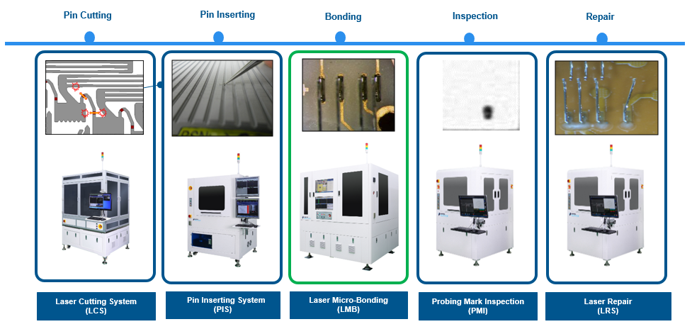
OVERVIEW
Korea's probe card assembly automation for DAWON NEXVIEW's probe card automation production line, from pin cutting, pin inserting, bonding, inspection and repair. Meet the needs of the entire probe card production line.
SPEC
SPEC
SPEC
BONDING PROCEDURE
This project is divided into two procedure. The transfer gripper is used to transfer the probes supplied to tray one by one to the pre-align zone. The bonding gripper is used to apply solder paste to the pre-aligned probe and arrange it on the ceramic substrate. Finally welding with Laser.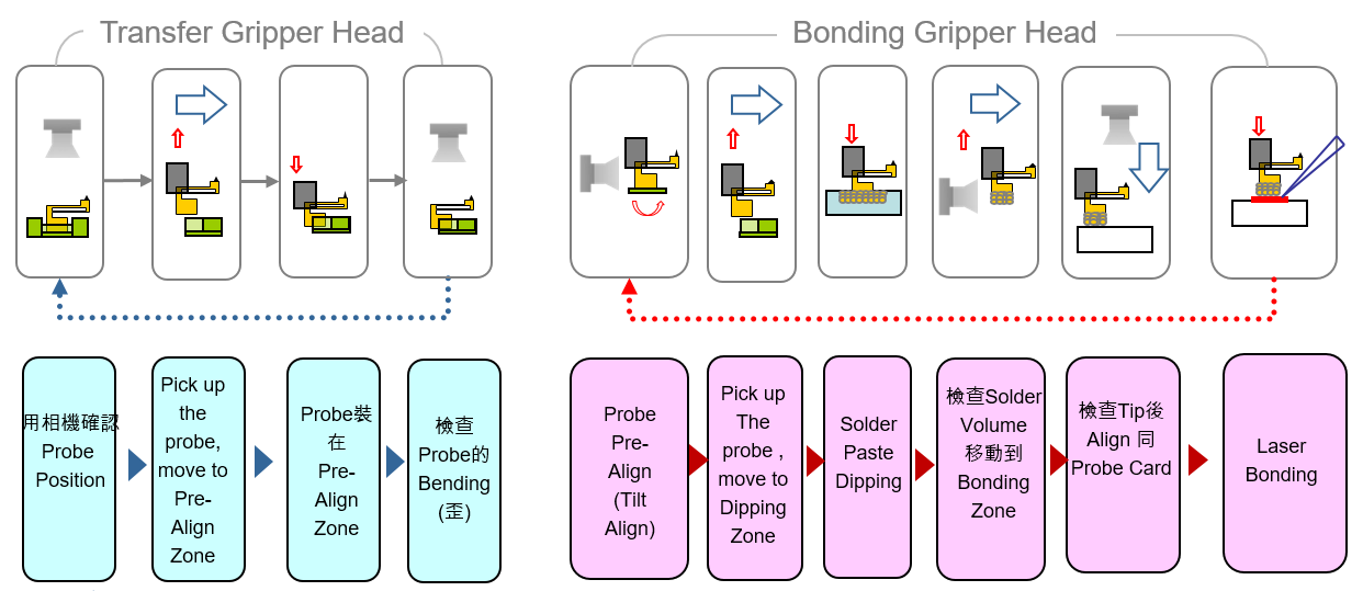
MACHINE STRUCTURE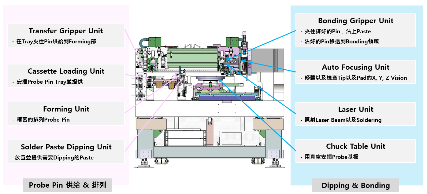
PROBE CARD TYPE
It is suitable for the manufacture of probe cards for DRAM, NAND FLASH, and CIS that require one-touch testing at the wafer level.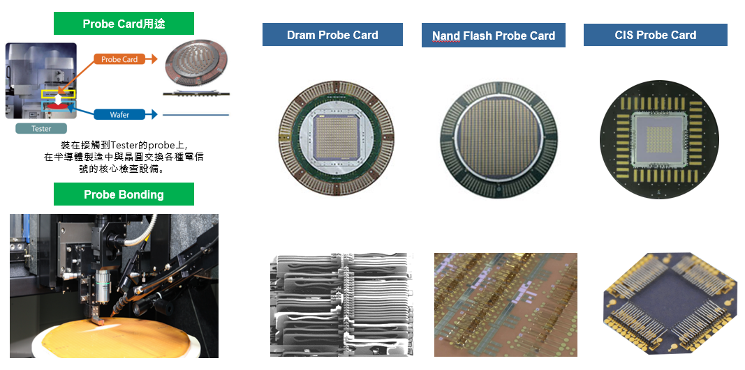
LASER PIN CUTTING SYSTEM
A device that vacuum-absorbs the probe pin wafer produced in the semiconductor engineering, and cuts and separates the connection part of each pin with a laser.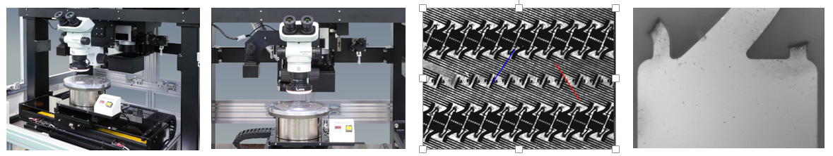
SPEC
| Equipped UV Nanosecond Pulsed Laser ( Picosecond Option) |
| Cutting Accuracy <±15μm |
| Cutting Time: <0.6sec/point |
| 4”, 6” wafer pin (8” , 12” Option) |
PIN INSERT SYSTEM
The cut probe pin is provided in dummy state or wafer state. The position is identified by vision, and it is automatically loaded to tray one by one.
SPEC
| High-speed work with Vacuum Picker Head and Inserting Gripper Head |
| Tact Time : < 5 sec / pin |
| Equipped High Precision Alignment Vision |
| 4”, 6” wafer pin (8” , 12” Option) |
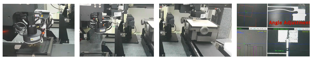
LASER MICRO-BONDING SYSTEM
After manufacturing wafers such as DRAM, NAND Flash, and CIS, in order to select defective products, it is a device for ultra-precision welding of tiny probe pins on the probe card substrate required for wafer-level testing.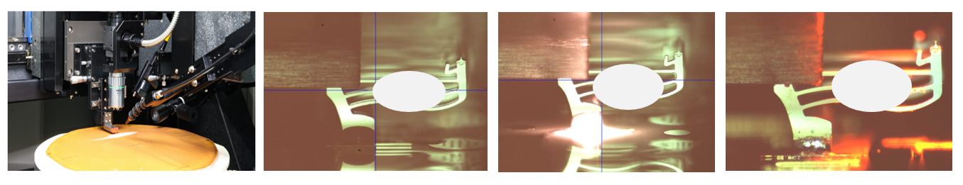
SPEC
| Bonding Accuracy ±5um (X, Y), ±8um (Z) within 300mm wafer |
| Less 10 sec/pin tact time @ standard bonding condition |
| Equipped Auto focusing Camera |
| ±1um position repeatability |
| 60um pitch bonding |
BONDING PROCEDURE
This project is divided into two procedure. The transfer gripper is used to transfer the probes supplied to tray one by one to the pre-align zone. The bonding gripper is used to apply solder paste to the pre-aligned probe and arrange it on the ceramic substrate. Finally welding with Laser.
MACHINE STRUCTURE
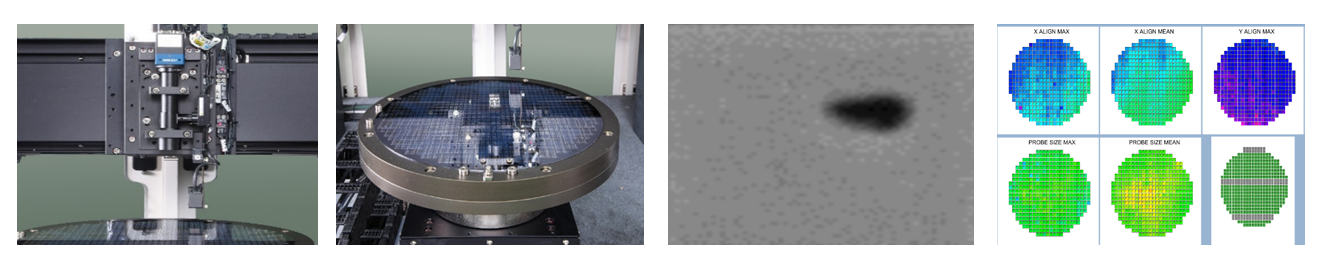
PROBING MARK INSPECTION SYSTEM
In order to confirm the final quality of the assembled probe card, after linking the probe card to the wafer, vision checks the remaining probe marks after the link to determine the quality of the equipment.
SPEC
SPEC
| 0.1 sec/mark Fast Inspection Speed |
| Probing Mark X, Y Deviation and Dimension Inspection |
| Provide Various Analysis Report |
| High Resolution 5M B/W CCD Camera (2,464 X 2,056 Pixels) |
| Less 0.1um Pixel Resolution (FOV 2.1 X 1.8 mm) |